New possibilities in diamond tool machining
with nano- and femtosecond lasers
When Theodore Maiman developed the first laser in 1960, no one initially knew what to do with the invention. "A solution looking for its problem," Maiman is said to have said about his invention. A good 60 years later, it is impossible to imagine modern manufacturing technologies without lasers. Today, lasers are synonymous with fast, contactless and thus wear-free processing with light.
For a long time, diamond could only be machined with great effort using other diamond tools, but the use of modern nano- and femtosecond laser technology now enables new possibilities in the machining of diamond tools.
Lasers have become an indispensable tool in the machining of diamonds today. For about 20 years, Nd:YAG lasers have been used to cut and mark rough diamonds into the right shape quickly and, above all, efficiently. In the production of diamond tools from polycrystalline diamond (PCD), green high-power lasers are used alongside wire EDM machines to separate PCD inserts for indexable inserts from blanks. Likewise, the use of modern laser technology in recent years has also revolutionized the shaping and grinding of PCD and CVD (chemical vapor deposition) diamond, as well as CBN (cubic boron nitride) inserts. Here, Q-switched nanosecond lasers replace both processes with just one operation. As a result, the use of laser technology saves valuable machining time and, above all, tool costs, since neither EDM wires nor diamond grinding plates are needed anymore.
Just a few years ago, this was the end of the manufacturing process for a classic indexable insert. Today, the new focus of tool manufacturers is on the production of complex, three-dimensional structures in PCD, which, as chipbreakers and chip grooves, enable new records in the metal removal rate year after year.
The first cutting tests with PCD at Innolas Photonics already date back around 10 years. However, since the market launch of the green 40W Blizz laser in 2017, global interest in this laser for diamond processing has increased continuously. This is due in particular to the Blizz lasers' unique combination of pulse energy, pulse duration and repetition rate, producing a peak pulse power of around 70kW at 1mJ and 15ns at 40kHz, making it virtually unrivaled. While other nanosecond lasers at 532nm with comparable or even higher average output power are optimized for high throughput and highly repetitive applications in microelectronics manufacturing, the Blizz is designed for short pulse widths while maintaining high pulse energies. As a result, the Blizz produces exceptionally high peak pulse powers, enabling high ablation rates in PCD that are -thanks to the short pulse duration- without a significant heat-affected zone. The Innolas Photonics Blizz laser thus offers a perfect combination of processing speed and process quality.
Not all PCD is the same
PCD consists of diamond powder in various grain sizes, which is sintered with cobalt to form a round blank. Cobalt serves as a catalyst and combines the mass to form an ultra-hard composite material with an extremely high thermal conductivity and an abrasion resistance around 500 times higher than that of hard metal. The grain size of the diamond powder, as well as the cobalt content, varies according to requirements and thus offers an optimum balance of wear resistance and hardness for machining a wide range of materials.
To find the optimum laser parameters for processing PCD, tests must therefore be systematically carried out with different PCD compositions. For this reason, PCD with different grain sizes in the range from 0.5 to 35µm, as well as different mixed grain sizes, were investigated in the tests carried out in the Innolas Photonics application laboratory.
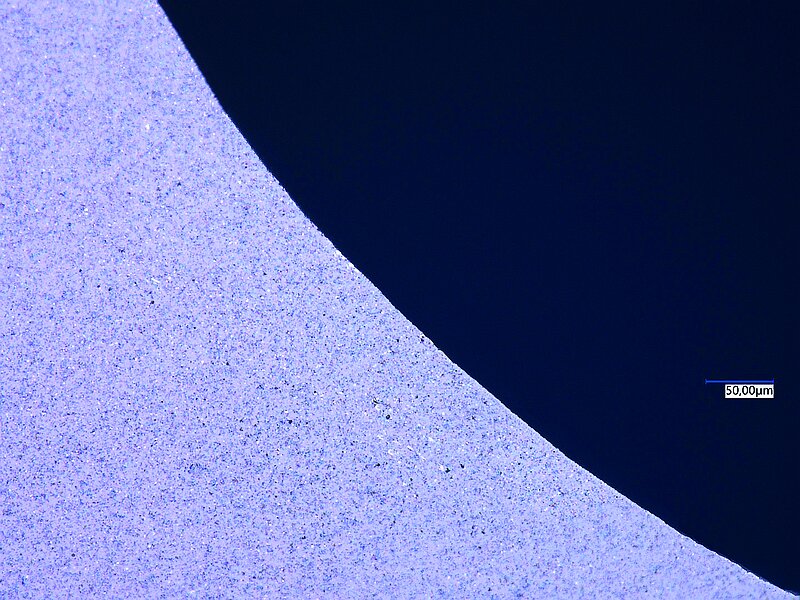
As expected, there was a clear difference in the possible cutting speed depending on the PCD composition. With 1.6mm thick PCD rounds from Diamonds, G. Wicke Handels-GmbH, for example, cutting speeds of up to 3.6mm/min were achieved. This corresponds approximately to the feed rates of the conventional wire EDM process. However, since the laser already produces roughnesses of less than 2.5µm at the cutting edge, the grinding processes downstream of the wire EDM process are no longer necessary, resulting in an enormous advantage in manufacturing speed.
Finest, high-precision structures thanks to femtosecond lasers
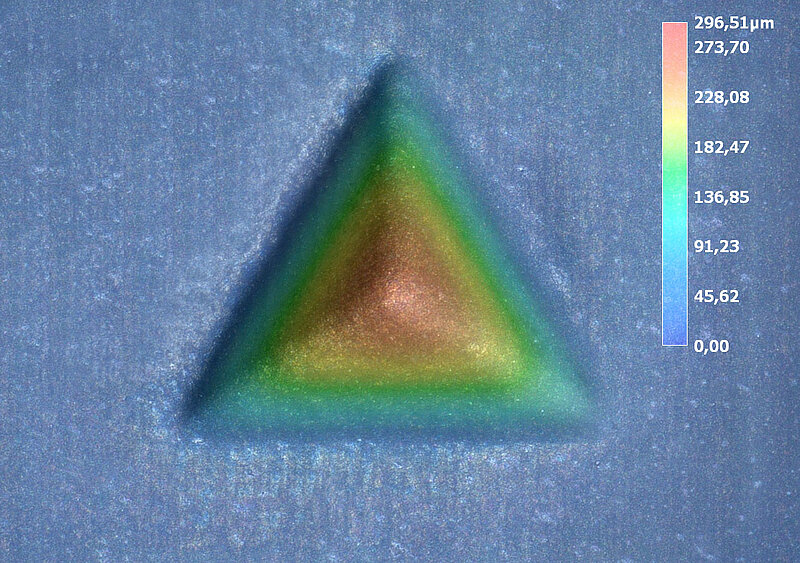
For the production of ultra-fine, high-precision structures in diamond, e.g. for the watch industry or for the manufacture of micro-milling cutters in the size range 50 to 300µm, a femtosecond laser is now increasingly being selected. With 60MW peak pulse power in 500fs short pulses, the Innolas Photonics Femto can play to its strengths perfectly here. The advantage of femtosecond lasers is obvious: no thermal effects, since the pulse durations are so short that the material has no time to heat up. Laser specialists refer to this as cold ablation.
In addition, the Femto enables the use of a so-called burst mode, in which several femtosecond pulses with a pulse spacing in the nanosecond range form a pulse package. The amplitude of the individual pulses within a burst can be varied at will, so that the enveloping pulse shape can be designed practically at will and optimized for the respective laser process.
To investigate the influence of burst operation on the ablation rate in more detail, the ablation rate on different PCD compositions was also investigated here as a function of different burst packages, burst shapes and for different average powers.
Laser frequency, scan speed, overlap and spot size were kept constant during the experiments. Figure 4 illustrates the results of the burst mode tests normalized to the ablation rate in standard pulse mode, Figure 5 the achieved cut edge quality.
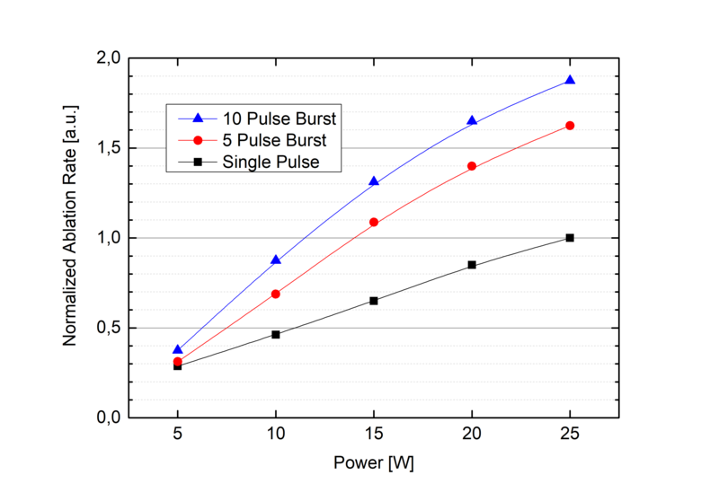
While in the lower power range the ablation rates of different bursts are still almost identical to those of single pulse operation, a doubling of the ablation rate is already achieved from 10W average power by using a burst of 10 in combination with optimized pulse intensities within the burst. The results thus illustrate the clear advantages of the femtosecond burst mode when ablating PCD, regardless of the PCD composition used.
New material compositions and laser-generated chipbreakers
The use of lasers in the machining of PCD means that it no longer has to be electrically conductive, a basic condition for machining by die sinking and wire erosion. This makes it possible to reduce the cobalt content in PCD or to partially replace it with other, electrically non-conductive materials. This opens up new possibilities for producing PCD compositions that are even harder than the mixtures known today. The laser process also makes it possible to generate virtually any cutting edge shape in PCD. While grinding wheels and wheels used to limit the shape of the cutting edges, the laser beam with a focus diameter in the micrometer range allows almost free shaping of the cutting edge. In this way, PCD tools with an inside corner radius of less than 5µm can be produced today. Likewise, the nano- and femtosecond lasers from Innolas Photonics enable contactless, selective ablation on the PCD surface and thus the precise production of extremely fine structures, e.g. for novel chipbreaker designs.
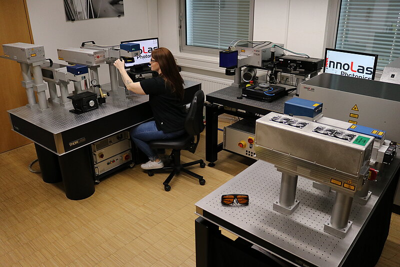
Welcome to the application laboratory
Customers as well as potential new customers are invited at any time to visit our application laboratory at our headquarters in Krailling near Munich and test which laser, in which mode of operation, is most suitable for the respective PCD material. With a laser portfolio in the wavelength range from 355 to 2000nm and pulse lengths from 500fs to 500ns, you will always find the right laser, even for the most demanding applications. However, our customers also benefit from the advantages of the Innolas Photonics nano- and femtosecond laser portfolio in other high-tech applications such as marking, trimming, structuring, PCB cutting, ID card production, additive manufacturing technologies, medical technology or photovoltaics.
Summary
The high pulse energy and peak pulse power of the Innolas Photonics Blizz laser not only enables rapid cutting of PCD including tungsten carbide carriers at speeds of up to 3.6mm/min, but also leaves perfect, clean cut edges with a roughness of less than 2.5µm, thus eliminating the need for grinding and polishing processes in the manufacturing process. By using the Femto, it is also possible to create highly precise, micrometer-fine structures in PCD, entirely without heat input into the material. The Femto Burst mode also makes it possible to increase the removal rates in PCD by a factor of two compared to the single-shot mode. Femto and nanosecond lasers thus open up new possibilities for the processing of PCD, as well as the generation of complex, high-precision structures for modern chipbreaker designs. Last but not least, both the inserts themselves and a wide variety of carbide tools can be heat marked with the same laser. And all this at virtually zero tooling cost, making the Blizz, like the Femto Laser, the perfect choice for any diamond tool manufacturer.