Innovative grinding technology is accelerating wafer processing
The semiconductor market is booming. Microchips are not only essential for electric vehicles and charging stations; they also play a significant role in solar and wind power plants and across the entire spectrum of communications technology. With expected growth rates of over 30 per cent per year, this multi-billion-euro market offers interesting prospects for grinding technology. At the GrindingHub trade fair, organised by the VDW (Association of German Machine Tool Manufacturers) from 5 to 8 May 2026 in Stuttgart, visitors can gain insights into manufacturing, machinery and precision grinding processes in the angstrom range. One thing is certain: if Europe wants to catch up with Asia and the US in the semiconductor sector, many things need to move faster, including the production process.
Wafers are thin discs that serve as the basis for the manufacture of microchips. The production of wafers involves several processing steps. In order to use silicon (Si) or silicon carbide (SiC) in the semiconductor industry, for example, it must be grown as a single crystal. The so-called ingots and boules are then machined into a blank disc. When cut into slices, these form the wafers, which are ground thin, polished and coated with an epitaxial layer to prepare them for the photolithography process. Using appropriate masks and light, circuit patterns are etched into the wafer. Finally, individual microchips can be cut from the wafer.
Significant growth potential

Michael Egeter, Vice President of Engineering at the Swiss machinery manufacturer Kellenberger
For Michael Egeter, Vice President of Engineering at the Swiss machinery manufacturer Kellenberger in Goldach, the steadily rising demand from end customers, along with new processes and technologies, makes a commitment to the semiconductor market seem thoroughly worthwhile. “In addition to the actual substrate processing – that is, the pre-grinding and preparation of raw crystals, and the creation of the wafer’s basic geometry – the field of semiconductor process equipment also offers good opportunities to provide grinding technology and solutions,” he says. Furthermore, grinding experts can put themselves in pole position with customers by offering bespoke solutions. Kellenberger has formed specialised customisation teams for this purpose. “Tailored solutions open up significant growth potential, particularly as they can often be scaled up,” emphasises the expert.
Don’t be afraid of (semiconductor) ceramics
Silicon carbide (SiC) is increasingly becoming the substrate of choice in semiconductor manufacturing. According to the Fraunhofer CSP in Halle (Saale), a semiconductor made from a compound of silicon and carbon offers a wide bandgap compared to a semiconductor made from pure silicon. This is a decisive factor for electrical conductivity and means that the semiconductor can be used under extreme conditions such as high temperatures, high voltages and high frequencies. For grinding operations, however, the substrate presents a challenge, as Michael Egeter notes: “We have already observed a certain degree of caution among grinders who have previously worked almost exclusively with metallic materials,” he reports. The machining behaviour of the grinding process on ceramics is completely different. Once this hurdle is overcome, the ever-expanding field of applications for technical ceramics and single-crystal semiconductor substrates will reveal itself as a huge potential for grinding technology.
SiC has already established itself as the gold standard in the semiconductor sector for certain power classes.
Egeter
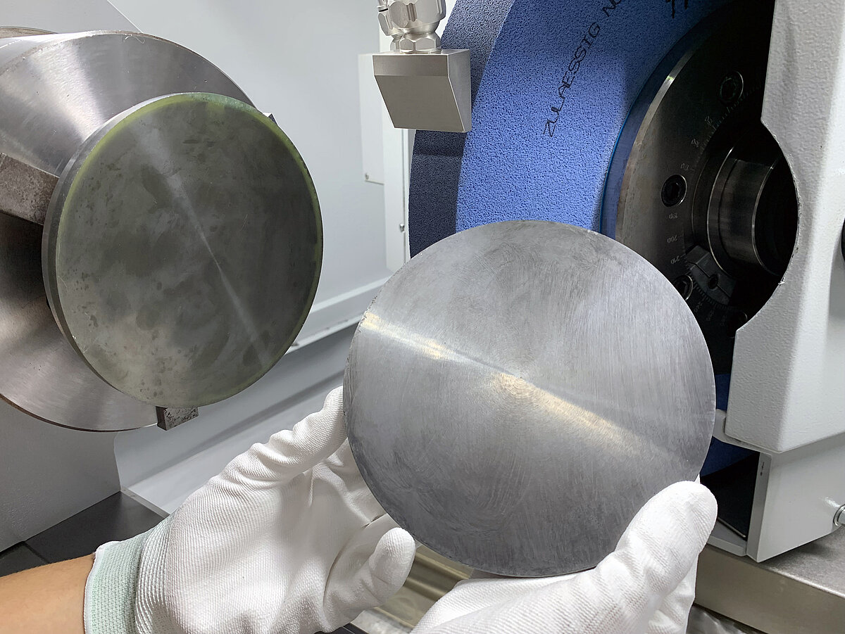
Manufacturing a puck is a challenge due to the hard and brittle nature of the material (SiC). The machining behaviour of the grinding process on ceramics is completely different from that on metallic materials
Save time in the manufacturing process
Semiconductor manufacturing is a time-consuming process. As a result, the delivery of chips requires a correspondingly long lead time, which poses a challenge for many sectors of industry. Even the raw crystal, which is grown in a high-temperature furnace at around 2,400˚C, takes a good two weeks before it can be shaped into a semi-finished product. For this so-called ‘ingot/boule to puck’ step, the Hardinge Group – to which Kellenberger belongs – formed a development team comprising engineers and application engineers, supported by SiC industry experts and raw material suppliers. The team analysed the inefficiencies in existing SiC ingot processing. The findings were incorporated into the development of an automated all-in-one 5-axis machine capable of machining all currently relevant specifications and diameters of SiC ingots. With automated loading and unloading, the machine can reduce the machining time for an ingot/boule into a puck – a process that takes more than 24 hours using conventional methods – to two to three hours, according to Kellenberger.
An ultra-fine challenge for grinding tools
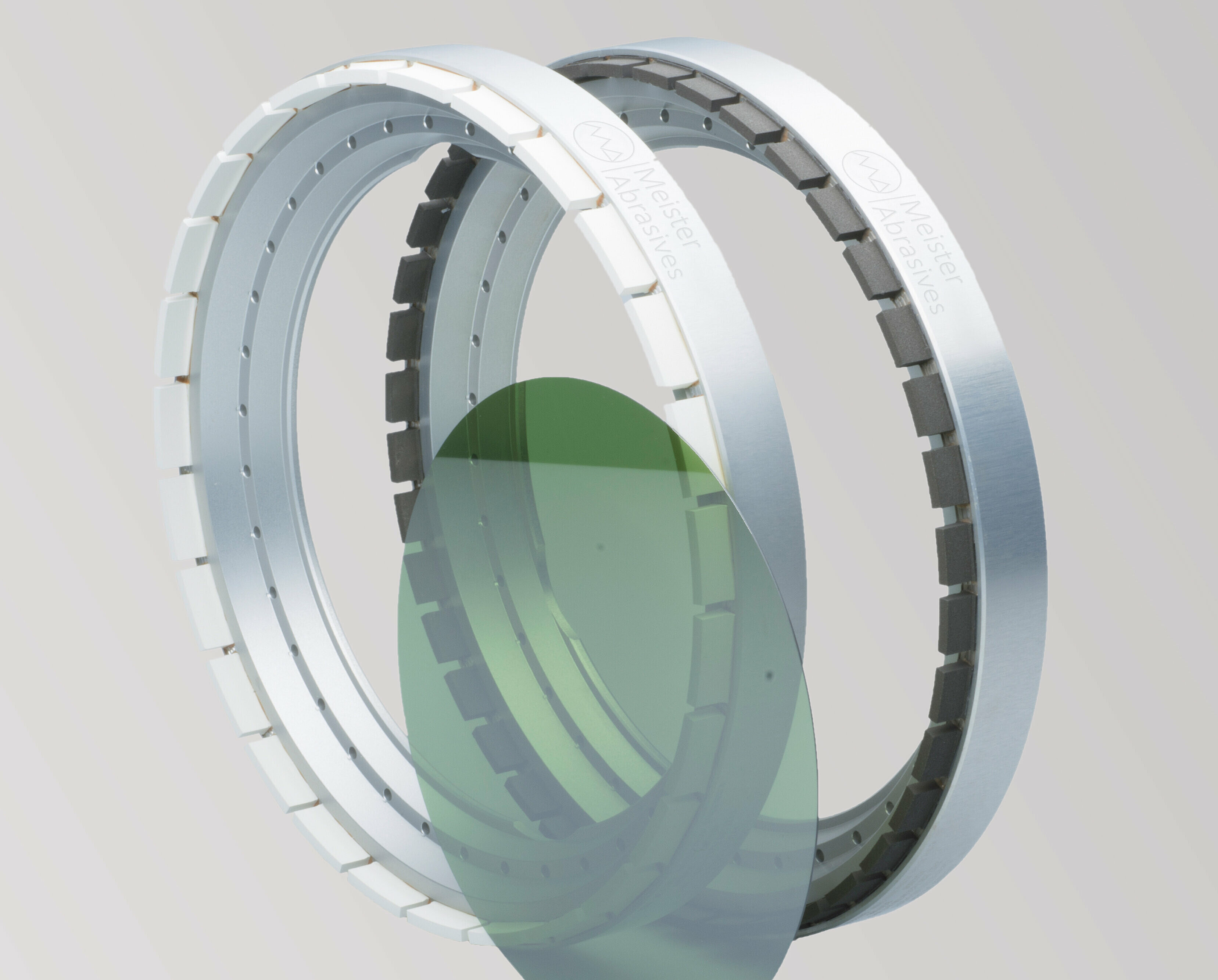
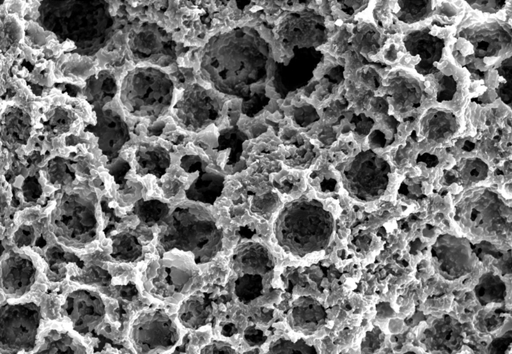
Alongside the substrate and the grinding machine, grinding tools play a crucial role in wafer processing. “We view the semiconductor sector as a rapidly growing market,” emphasises Carmine Sileno, Product Manager for the semiconductor division at Meister Abrasives. The company, based in Andelfingen, Switzerland, specialises – together with its German sister company Alfons Schmeier in Helmbrechts – in the development and manufacture of superabrasive grinding tools for high-precision grinding applications. For the various stages of the semiconductor manufacturing chain, from the raw crystal to the finished chip, Meister Abrasives offers solutions that customers in wafer or chip manufacturing can use on existing equipment. The diamond grinding tools developed for wafer surfaces ensure surface qualities in the range from Ra 5 Ångström (1Å = 0.0001μm). By way of comparison: a human hair has a diameter of 40–80 μm. Quality assurance at such high surface finish levels is only possible using white-light interferometry or atomic force microscopy (AFM), says Carmine Sileno. He is bringing wafers to GrindingHub as illustrative material, the surfaces of which can be examined under the microscope. “For chip manufacturers, uniform surfaces with homogeneous nano-topography are of enormous importance,” emphasises the product manager at Meister Abrasives. With its UltraFine technology, however, the Swiss company is also pursuing another goal: “We want to grind as finely as possible in order to shorten subsequent process steps or, ideally, eliminate them entirely,” says Sileno. This applies above all to time-consuming and costly lapping and polishing processes.
Carmine Sileno, Product Manager at Meister Abrasives
Eliminate individual process steps
Wafers are usually first ground and then polished to achieve the required high surface finish. The slurries used for polishing are mixtures of fine solid particles and a liquid. This polishing agent is expensive. “The longer a polishing process usually takes and the larger the wafer surface, the more appealing it becomes to minimise the polishing process as much as possible or eliminate it from the process altogether,” says the grinding expert. The greatest challenge in machining the hard wafer surfaces was developing the right bond for the sub-micron diamond grain (< 1 μm). This is precisely where Sileno sees Meister Abrasives’ strength: the ability to tailor the abrasive coating structure in detail for every application. By shortening or even eliminating polishing processes, the customer saves valuable time, reduces costs, requires less infrastructure and increases throughput.
Machining ultra-hard SiC wafers requires grinding wheels capable of achieving surface finishes in the single-angstrom range.
The biggest challenge in machining hard wafer surfaces was developing the right bond for the sub-micron diamond grain.
Source | VDW
Photos | Kellenberger AG, Meister Abrasives